Key learning points
- PCBs are manufactured using CNC machining or chemical etching
- CNC machining mills away copper using a CNC router and design software
- chemical etching uses UV light, photo-resist, and chemicals to remove copper
- CNC machining is safer and less wasteful, but slower
- chemical etching is faster and cheaper, but uses hazardous chemicals
- PCB design involves placing components, creating tracks and pads, and using design software
- PCB amendment involves updating components, modifying tracks, and repositioning pads
- PCBs are used for space-saving, reliable connections, ease of repair, and professional appearance
Manufacturing printed circuit boards (PCBs)
There are two main ways to manufacture printed circuit boards (PCBs):
- CNC machining
- Chemical etching
PCB manufacture using CNC machining
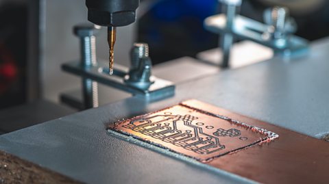
Using a CNC milling machine to mill away the unwanted copper to create a circuit board
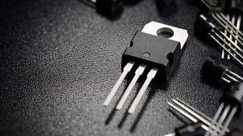
Tools required: Computer with PCB design software, CNC router and copper-clad board
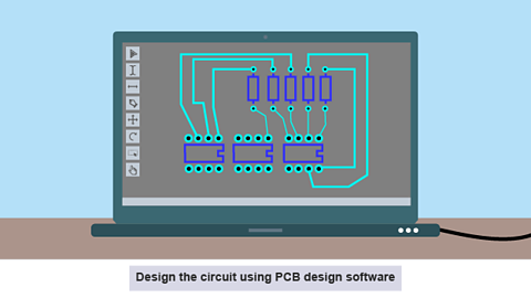
Image caption, Design
1 of 6
Process:
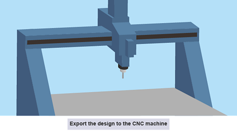
- Design the circuit using PCB design software
- Export the design to the CNC machine.
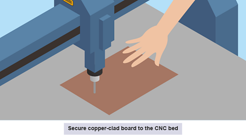
- Secure copper-clad board to the CNC bed.
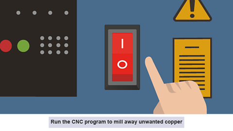
- Run the CNC program to mill away unwanted copper.
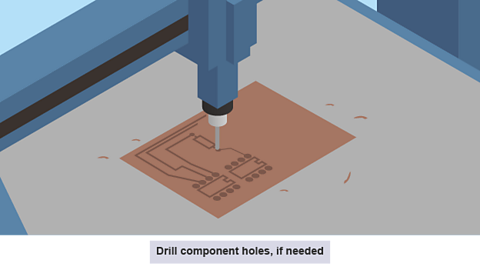
- Drill component holes, if needed.
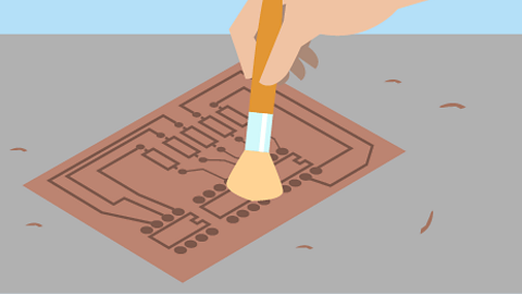
- Clean the board to remove debris.
- Pros: safer, no chemicals, less waste
- Cons: slower for complex designs
PCB manufacture using chemical etching
Using a chemical method to remove the unwanted copper to create a circuit board.
Tools required: UV light box, photo-resist board, developer solution and an etching tank.
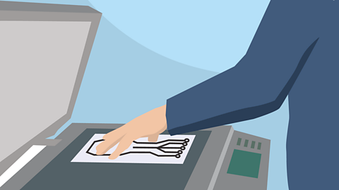
Image caption, Copy
Photocopy or trace a copy of the circuit onto an acetate sheet to make a mask of the circuit. This is called the PCB Artwork.
1 of 6
Process:
- Design the circuit using PCB design software. Print the design onto a transparency/acetate sheet. This is called the PCB artwork
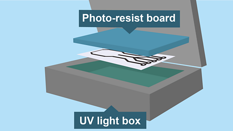
- Prepare the photo-resist board by peeling off the protective film. Place the transparency on the photo-resist board. Expose to UV light in a light box (approx 3 minutes)
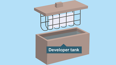
- Develop the board in Sodium Hydroxide solution (about 10 seconds). Rinse the board with clean water
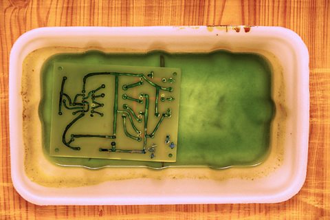
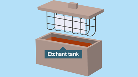
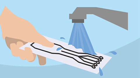
- Place in a heated etching tank of Ferric Chloride (15-45 minutes). This will remove unwanted copper. Remove and rinse when etching is complete.
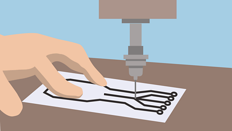
- Drill component holes with a PCB drill
- Pros: faster for multiple boards, cheaper
- Cons: uses harsh chemicals, more environmental concerns
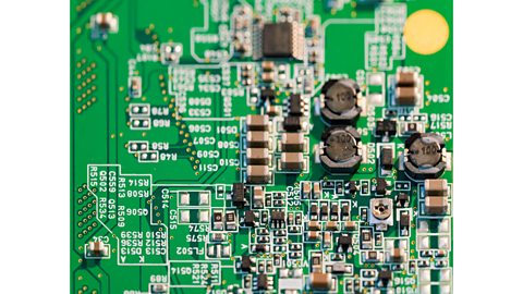
Why use PCBs?
- space-saving compared to just using components soldered using loose wires
- easier to repair - just swap components
- more reliable connections
- professional appearance
Electrical safety in circuit production
When working with printed circuit boards (PCBs) or A breadboard is a plastic board with a grid of holes that allow you to connect electronic components without soldering. Useful when prototyping circuits., it's crucial to stay safe. Here are the key hazards to watch out for:
short circuits:
- double-check connections before powering on
- use insulated tools to avoid accidental shorts
- keep metal objects (like paperclips) away from live circuits
component damage:
- handle components gently, especially integrated circuits (IC)
- be aware of static electricity
- check polarity of capacitors and diodes before inserting
burns:
- let soldering irons cool completely before storing
- be careful with hot components after extended use
chemical exposure (for pcb etching):
- wear gloves and eye protection
- work in a well-ventilated area
- dispose of chemicals properly
Tidy workspace = safer workspace.
Keep things organised and you'll reduce risks!
Test yourself
More on Electronic control systems
Find out more by working through a topic
- count3 of 8

- count5 of 8
- count6 of 8